

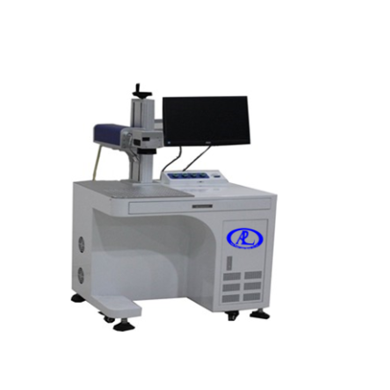
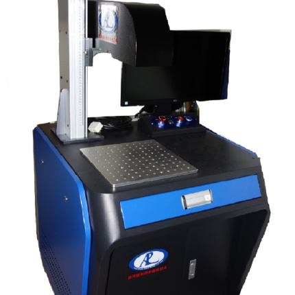
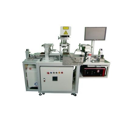
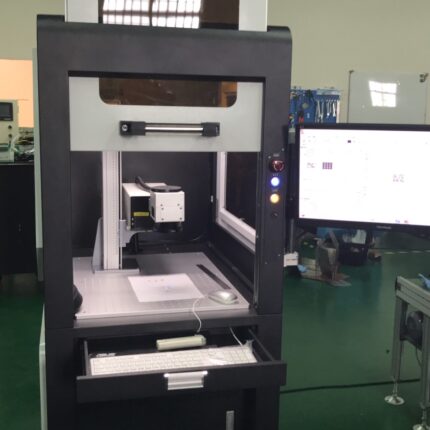
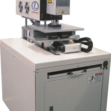
Program advantage
The traditional PCB industry adopts press-bonding or high-temperature sintering, and then etches into the final line through exposure and development, which not only causes a large amount of waste of materials, but also problems such as schedule, product accuracy, productivity and pollution. With laser processing technology, high-quality PCB boards can be obtained quickly, energy-efficiently and without pollution.
1. The laser processing method is non-contact processing, and the heat affected zone of the component is small during the processing.
2. The laser processing and molding is more elaborate, reaching the micron-level processing, and its superiority is particularly prominent in the micro-hole fabrication and the different formation of the electronic circuit board.
3. The laser processing accuracy is high, the laser beam diameter can be less than 10μm, and can be ultra-fine processing. It is non-contact machining with no obvious mechanical force, which is easy to locate and ensure high machining accuracy.
4. The wide range of laser processing materials, suitable for processing a variety of metal and non-metallic materials.
5. The laser processing performance is good, there is no special requirement for the processing occasion and working environment, no vacuum environment, no radioactive ray, no pollution. Laser processing speed, efficiency, flexibility and simplicity.
Reviews
There are no reviews yet.